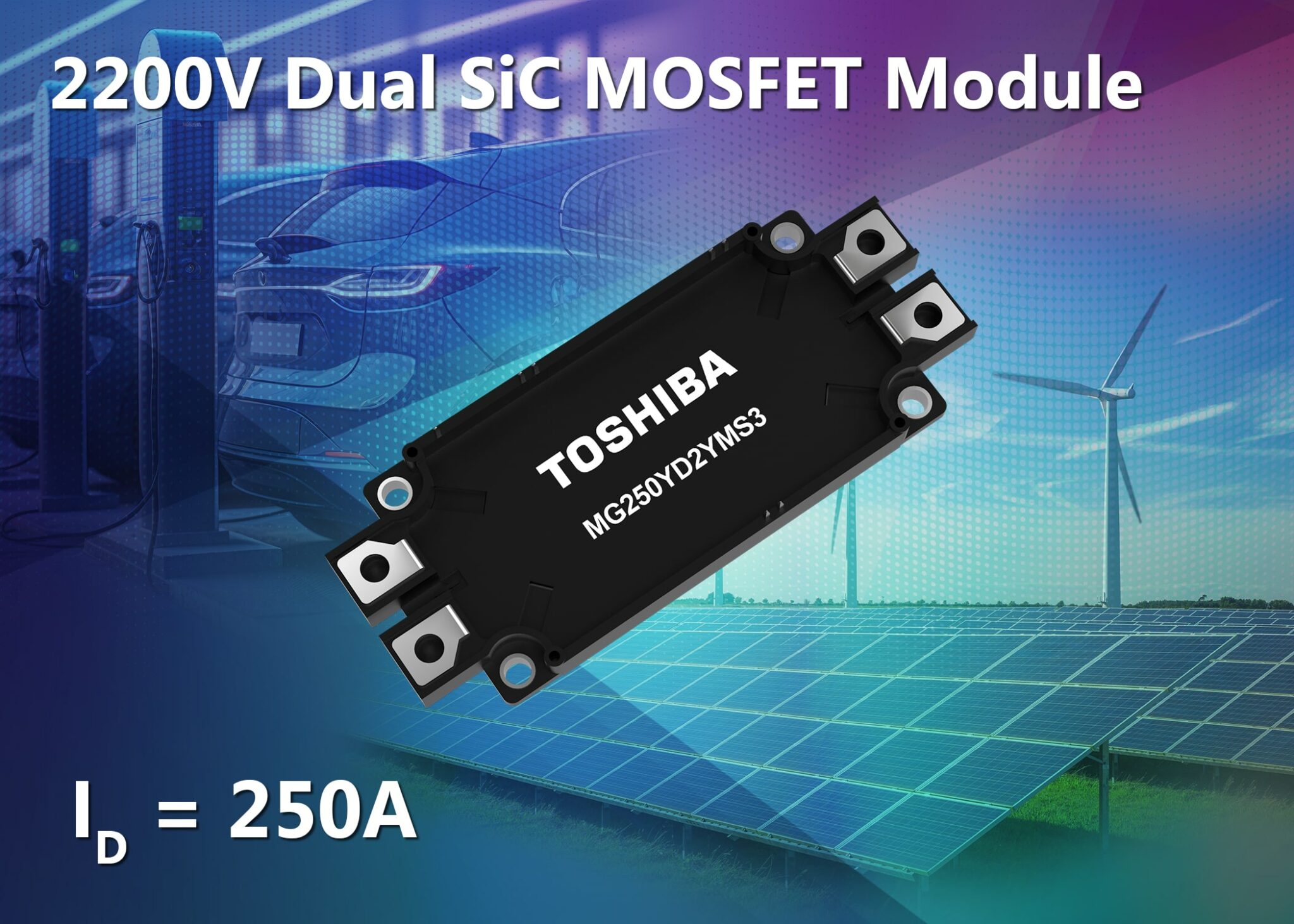
Dual SiC MOSFET module enables low loss, high-performance two-level inverters.
Toshiba Electronics Europe GmbH (“Toshiba”) has developed a new 2200V rated silicon carbide (SiC) MOSFET with embedded Schottky barrier diode (SBD) for use in 1500V DC applications such as photovoltaic (PV) inverters, electric vehicle (EV) chargers, high frequency DC/DC converters and energy storage systems. The new device will simplify inverter designs and increase power density, thereby reducing size and weight.
Conventional three-level inverters exhibit low switching losses as the off-state voltage across switching devices is half the line voltage. In comparison, two-level inverters have fewer switching modules making them simpler, smaller, and lighter. However, they require semiconductor devices with higher breakdown voltage, as the applied voltage is the line voltage. Meeting this challenge is important as a two-level inverter based upon the new device achieved higher frequency operation and lower power loss than conventional three-level silicon (Si) IGBT inverter.
The new dual SiC MOSFET module (MG250YD2YMS3) has a VDSS rating of 2200V and is capable of supporting a continuous drain current (ID) of 250A, with 500A in pulsed operation (IDP). Isolation (Visol) is rated at 4000Vrms and the device can operate at channel temperatures (Tch) as high as 150ºC.
It offers low conduction loss with a typical drain-source on-voltage (VDS(on)sense) of 0.7V. Switching losses are minimized with typical turn-on and turn-off losses of 14mJ and 11mJ respectively, meaning that the requirement for thermal management is less, resulting in smaller inverters.
Within the MG250YD2YMS3, the impurity concentration and thickness of the drift layer have been optimized to maintain the same relationship between the on-resistance (RDS(ON)) and the breakdown voltage as existing products. This also strengthens immunity to cosmic rays, a key requirement for PV systems. Furthermore, embedding SBDs with clamped parasitic PN junctions between the p-base regions and the n-drift layer ensures reliability in reverse conduction conditions.
Switching energy loss for the developed all-SiC module is far lower than equivalent silicon modules. In comparison, the new SiC module achieves double the frequency of a conventional Si IGBT, as well as 37% lower loss when comparing a two-level SiC inverter against a three-level Si inverter.
Shipments of the new device will start in September 2023.
For further information, please visit: https://toshiba.semicon-storage.com/eu/semiconductor/product/mosfets/sic-mosfet-modules/detail.MG250YD2YMS3.html