Excellent thermal performance and significantly reduced parasitic effects characterize Infineon’s OptiMOSTM power MOSFETs.
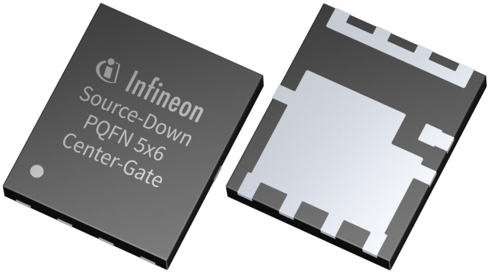
Infineon’s OptiMOSTM power MOSFETs with 25 V to 150 V are now available at Rutronik as an improved version in the source-down package with bottom-side cooling and center-gate footprint. They have been optimized especially for applications where parallel connection is necessary and have the lowest possible on-resistance RDS(on) on a 5 mm x 6 mm PCB area. The OptiMOSTM family also features significantly reduced package parasitics and excellent thermal performance. The transistors are RoHS-compliant and available in reel packaging at www.rutronik24.com.
The main feature of the source-down package concept is the orientation of the active side of the silicon chip to the bottom of the component. Combined with the reinforced clip on the top of the silicon chip, package parasitics are significantly reduced while thermal performance is taken to the next level. State- of-the-art silicon technology with excellent FOM and maximized chip / package ratio increases current capability and ensures minimized power losses. Infineon’s OptiMOSTM power MOSFETs enable fast switching and reduce the need for parallel switching of components.
Key functions at a glance
- Minimized line losses
- Reduced voltage overshoots
- Increased maximum current carrying capacity
- Fast switching
- Less parallel connection of components required
Examples of applications:
- Robotics
- Solar
- Telecommunications
- Low voltage drives
- Light electric vehicles
- Drones
- Electric tools
- Battery Management System
- Class D audio applications USB