LDS enables the production of electronic assemblies with flexible geometric shapes. This process enables electronic products (such as smart phones, sensors or medical devices) to become even smaller and more powerful. Automated manufacturing processes also make this process more economically attractive.
There is less and less space available for electronic assemblies, so solutions are needed which replace conventional printed circuit boards. LDS enables further miniaturisation and makes increasingly complex geometric designs possible. This is a stable and reliable process that has established itself in quality-critical sectors such as medical technology or safety-relevant components for the automotive industry.
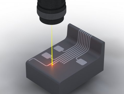
The LDS process enables three-dimensional assemblies
Direct laser structuring enables 3D-MID (Mechatronic Integrated Devices) assemblies to be produced. When using 3D-MID, electronic components can be fitted directly onto a three-dimensional base body, without circuit boards or connecting cables. The base body is manufactured using an injection moulding process, whereby the thermoplastic material has a non-conductive, inorganic additive.
The additives in the material are “activated” by direct laser structuring so that the plastic material can accommodate the electrical conductor paths. The laser beam writes the areas intended for the conductor paths and creates a micro-rough structure. The released metal particles form the nuclei for the subsequent chemical metallisation. In this way, the electrical conductor paths are applied to the areas marked by the laser. The other areas of the three-dimensional base body remain unchanged. The plastic component can then be assembled in standard SMD processes similar to a conventional PCB. It is also suitable for soldering in a reflow oven.
Versatile application of laser technology
HARTING 3D-MID AG is the largest supplier of 3D-MID components outside of Asia. HARTING uses high-performance laser systems for the LDS process, with three lasers working in parallel, each offset by 45 degrees. Thanks to an additional axis of rotation, components can be processed by the laser simultaneously from all sides (360 degrees). This technology enables flexible geometric shapes, such as reflector shells or LED lights, to be made. Despite the minimal conductor path thickness of 16 to 20 μm, the conductor paths are still suitable for demanding automotive components or for applications with currents up to 10 A – for example for heating coils in cameras which are used to prevent the optics from fogging up.